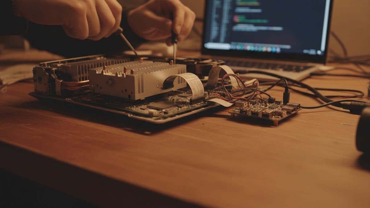

Huawei shows 7.2 Tbps optical module to accelerate AI clusters
Near-package optics technology places optical components next to the switching chip to cut signal loss and power consumption. It's still under development.


Huawei presented what it calls the industry's first near-package optics (NPO) module with a throughput of 7.2 terabits per second, aimed at AI infrastructure. The information was published by TechNode, based on a report from the South China Morning Post.
The round number hides an architecture decision that matters to anyone who builds or operates training and inference infrastructure: where to place the optics relative to the chip. Let's get into what the announcement actually means.
What Huawei showed, in numbers
The module combines 36 channels operating at 200 Gbps each, which results in the 7.2 Tbps of aggregate throughput (36 × 200 = 7,200 Gbps). The company made clear that the product is still under development and that volume production will depend on supply chain and manufacturing readiness.
| Item | Value |
|---|---|
| Aggregate throughput | 7.2 Tbps |
| Number of channels | 36 |
| Speed per channel | 200 Gbps |
| Stage | Under development |
| Volume production | Depends on supply chain/manufacturing |
It's important to separate marketing from technical fact: Huawei didn't announce commercial availability. It announced an engineering demonstration. For the reader planning infrastructure, this shifts the adoption horizon from "you can already buy it" to "worth keeping an eye on."
Why "near-package" changes the game
In an AI cluster, the bottleneck that limits performance is rarely just the GPU. It's the interconnect between thousands of accelerators. When a large model is split across hundreds of chips, those chips need to constantly exchange gradients and activations, and the network becomes a bottleneck in both latency and energy.
Historically, optics sit in pluggable transceivers at the edge of the switch (the pluggable architecture), far from the chip. The electrical signal travels a relatively long distance from the die to the optical module, which generates signal loss and forces higher energy spending to compensate.
The idea behind near-package optics is precisely to shorten that path: placing the optical components closer to the switching chip. According to TechNode, this reduces signal loss and power consumption as AI clusters connect more processors. It's an intermediate step in the same direction as what the industry has been calling co-packaged optics (CPO), in which optics are integrated even more tightly with the chip.
In practice, the difference between these approaches translates into three axes that operators feel in their wallets:
- Energy per bit transmitted, which dominates operational cost in AI data centers;
- Bandwidth density per switch, which defines how many accelerators you can connect within the same domain;
- Network latency, which affects synchronization time in distributed training.
The context the announcement doesn't tell
This launch doesn't happen in a vacuum. Huawei operates under export restrictions that limit its access to the most advanced GPUs on the Western market. In light of that, the company's strategy has been to compensate for individual chip limitations with scale and interconnect: if you can't have the fastest accelerator, you connect more accelerators more efficiently. A very-high-bandwidth optical module with low power consumption is a central piece of that bet.
The announcement also connects with another goal announced by China on the same day: reaching 9,800 EFLOPS of intelligent computing capacity by 2030. Efficient interconnect is a prerequisite for that kind of goal, because adding up FLOPS is pointless if the network can't keep up.
It's worth registering healthy skepticism: for now, what exists is the demonstration of a module and a claim of pioneering status ("industry first"). There are no independent public benchmarks, no price, and no date. TechNode reports what Huawei said, and the company itself conditioned volume production on the supply chain.
What this changes for the Brazilian developer
This is where the view needs to be honest. You, who train or run models, won't buy this module anytime soon, and probably never directly. The impact is indirect but real, and comes through two paths.
1. Cloud and inference cost. The cost of running large models is dominated by infrastructure, and interconnect is a significant part of an AI data center's energy cost. Technologies that reduce energy per bit and increase bandwidth density push the cost per inference token down over time. If you pay for a model API or rent GPU in the cloud, the evolution of data center optics is at the bottom of your bill, even if you never see it.
2. Supplier diversity. One of the structural risks for anyone building a product on top of AI today is concentration. The more manufacturers push the interconnect frontier, including players outside the Western axis, the greater the chance of more training and inference capacity supply in the global market in the medium term. For Brazil, which imports practically all of its advanced computing capacity, competition at the infrastructure layer tends to be good news for pricing.
What doesn't change in your day-to-day: nothing in your code, nothing in your stack, nothing in how you write a training loop or configure a cluster today. This is a move at the physical layer, far from the API you call.
What remains open
The questions worth following over the next few months:
- When (and if) the module goes into volume production, since Huawei itself conditioned that on the supply chain;
- How it compares to co-packaged optics solutions from other manufacturers in energy per bit and cost;
- Whether independent benchmarks appear confirming the 7.2 Tbps under real cluster conditions, and not just in a demonstration.
For now, the concrete data point in hand is this: 36 channels of 200 Gbps, optics placed right next to the switching chip, still under development. It's a clear signal of the direction AI infrastructure is taking, with the interconnect moving away from the switch edge and getting closer and closer to the silicon. For anyone building software on top of AI, it's one more reminder that tomorrow's bottleneck isn't just the GPU, it's the (optical) wire between them.
Translated from the Brazilian Portuguese original · Read the original

OpenCode suffers breach, triggers unauthorized charges on users' AI accounts
OpenCode, an open-source coding agent that has been gaining ground as an alternative to Claude Code and Cursor, confirmed a breach that exposed API keys belonging to some users of its online platform. The case also exposed a bigger problem: security teams struggle to use commercial AI models in incident response, because the models' own safety defenses block analysis of malicious code.